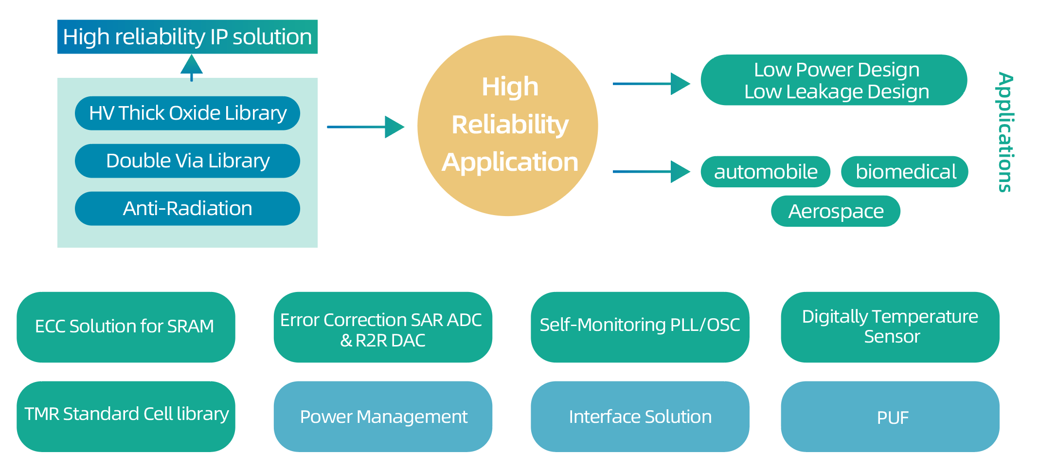
High reliability IP and chip design services
When chips are used in automotive, medical and industrial applications, the most important requirement is reliability, which requires a design perspective to solve potential defects that may occur during the manufacturing process. These manufacturing defects may not manifest themselves in the early stage of the product, but may cause circuit failures within the chip after a period of use. Therefore, we have developed two sets of standard cell libraries for high-reliability chip design solutions that can be widely applied in automotive, medical, and industrial products.
The first set is the "Thick Gate Oxide Standard Cell Library," designed by using transistors with a thick gate oxide layer in the manufacturing process.
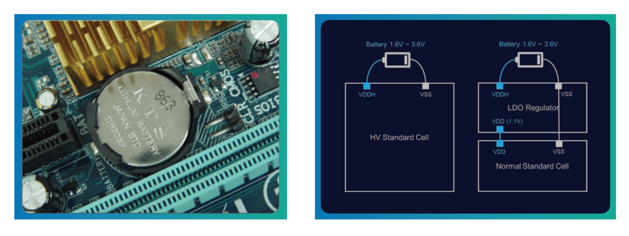
There is an oxide layer between the gate and the current channel of a transistor. We can control the formation of current channel by applying varying voltages to the gate, thus turning the transistor on or off. Because the thin oxide layer beneath the gate may be damaged after the prolonged use of the transistor, leading to a leakage current path between the gate and the current channel of a transistor. It is reflected on the chip as an increase in component leakage current and a decrease in component controllability. Therefore, increasing the thickness of the gate oxide layer can effectively prevent the formation of such leakage current path, thereby improving the reliability of the chip.
In addition, components with thick gate oxide layer have higher voltage tolerance, low leakage currents, and a higher ability to resist power noise.
We offer 221 standard cells with thick gate oxide. Compared to the standard cells offered by wafer foundries, ours reduce leakage current by over 60% and improve power consumption issues caused by 80% of power noise.
The second set is the "Double VIA/CONTACT Standard Cell Library," which leverages circuit layout skills and design capabilities to effectively strengthen the internal connections of transistors by adding extra vias within the standard cell provided by wafer foundries.
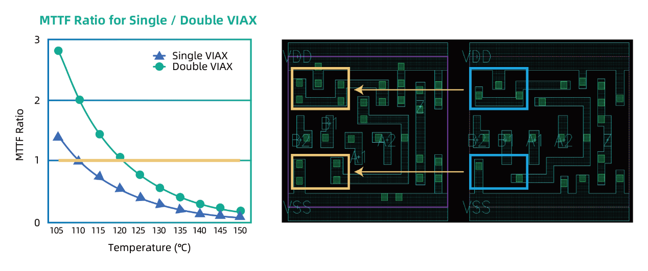
Vias (or contacts) are the connection material between the conductive layers inside a transistor, and it is very small in size. During the wafer processing, environmental particles are an inevitable source of contamination. If these particles fall into the vias, they will form a high-resistance conductive path, causing heating and premature aging or slower operation of the transistor, and making chip malfunction more likely. However, by adding additional vias, we can effectively improve process defects caused by environmental particles.
Compared with standard cells provided by wafer foundries, 753 double vias/contacts standard cells we provide can more than double the mean time to failure (MTTF) even at high temperatures of 125 degrees Celsius. The increase in MTTF represents an increase in reliability. Therefore, our technology is particularly suitable for designing automotive, medical and industrial chips.