Lingyange's chip design service platform (DSP: Design Service Platform) offers integrated one-stop services from chip design, functional verification, prototype verification, physical design optimization to mass production manufacturing.
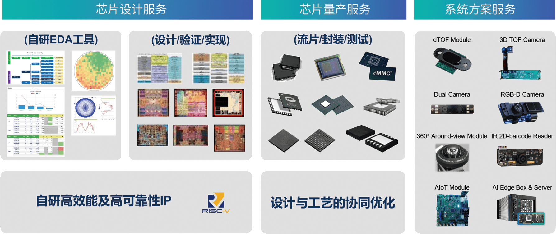
Assist industry customers from product design, chip design to chip mass production, industry standard certification to system landing, providing one-stop integration solutions.
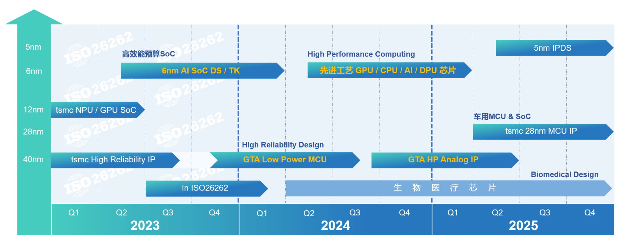
● In 2023, ISO26262 process certification introduced, and 40nm high reliability basic IP development implemented.
● In 2024, officially enter the field of biomedical and continue the 6nm advanced process project.
● In 2025, will develop 40nm high-performance analog IP, enter the MCU reference design platform and IP development.
To achieve the needs of customers, complete the complex process from the hair to the chip launching. From customer application scenarios to chip specifications, from netsheet design to GDS streams, including IP Sourcing services, physical implementation, timing closure, Test circuit insertion (DFT insertion) and reliability verification. We also provide analog IP and standard library IP customization services. In the process and chip design co-optimization service, we provide complete software and hardware solutions, from the IP of the wafer manufacturing variation detection system to the corresponding analysis software, to help improve chip performance and yield. Lingyange also provides EDA reference design process to solve the design and manufacturing problems of chip design companies.
Diversified IP solutions
Lingyange's chip design service platform provides IP customized design services, professional IP procurement (ARM CORE, high-speed interface: PCIe, DDR, etc.) and design integration.

Customized basic IP design
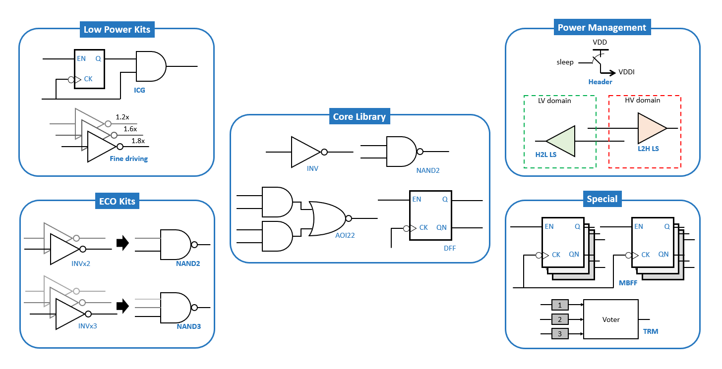
Our comprehensive design system optimizes the performance of various design architectures, helping designers meet stringent power and area requirements while reducing integration risks. The customized low voltage component library can effectively balance the power consumption and performance requirements of the product, suitable for high performance, low power, low leakage and high density component library product applications. The customized multi-critical voltage module library can effectively suppress the leakage current balance performance and leakage current requirements, and is widely used in low-power products to balance performance and long-term standby system requirements. The library of highly reliable components is tailored to meet the needs of industrial and higher levels of reliability in a wide range of demanding applications, and is widely used in low-power, energy-efficient computing. Component libraries with different specifications.↓
Customized IP
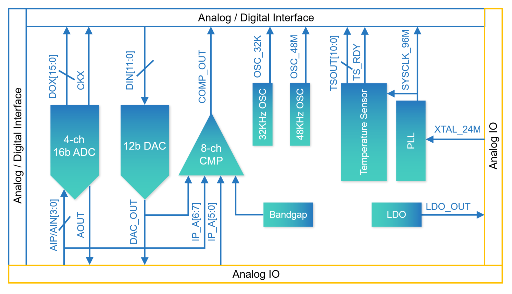
●Digital-to-Analog conversion circuits with various architectures (SAR, Sigma-Delta, R2R) and different accuracy (10~16 bits);
● All kinds of Oscillator IP (Oscillator, PLL, DLL);
● All kinds of power related IP (POR, LDO regulator, Bandgap reference)
● Full digital temperature sensor
Front-end chip design services

* Including RTL design synthesis, DFT, DV design verification and other services.
Back-end chip design services

* Including APR layout, PV verification, timing and reliability verification and other services.
Chip manufacturing service
Package design and testing - mass production services
Packaging Design
● Evaluation and recommendations for each package type
● Package/welding wire/substrate layout design
●SiP package evaluation and optimization
● Electrical/thermal/mechanical performance simulation and optimization
● Engineering support for package process development
● Package failure analysis and continuous improvement
● Mass production data analysis and factory management
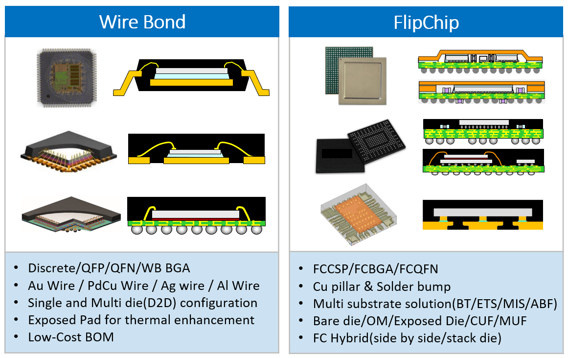
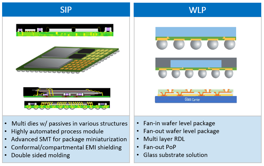
Available package types ▼
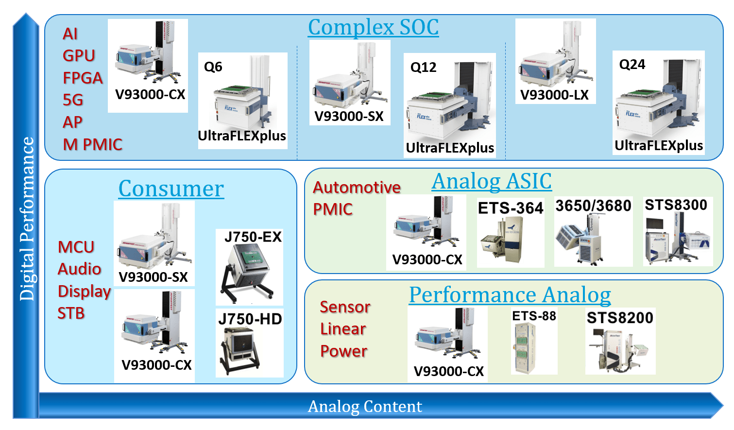
Testing Development
●Provide one-stop test program development and mass production management services for wafer (CP) and finished product (FT).
● Based on customer product characteristics, we provide V93K, UltraFLEX, J750, Chroma, AccoTest, Nagawa and other corresponding platforms to meet customer quality, cost and efficiency requirements.
● Synchronous chip development time, MPW stage for BIST, DFT, DFM and other verification.
● The SLT test technique is brought into the FT test to test the highly integrated chip.
●SPAT, DPAT, GPAT processing methods to meet the needs of industrial control, vehicle regulation level.
● Mass production yield control and yield improvement.
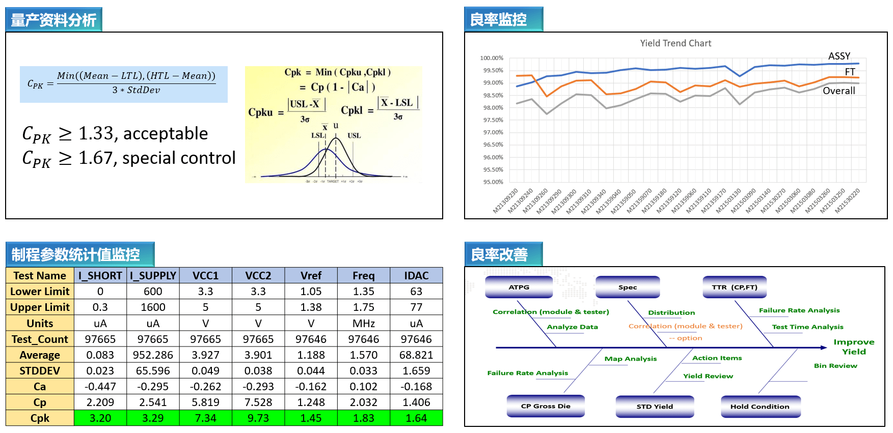
Mass production process management system PDAS
Self-developed process capability management system to monitor the yield of production lots and the statistics of key measurement parameters.
Collaborative optimization of design and process
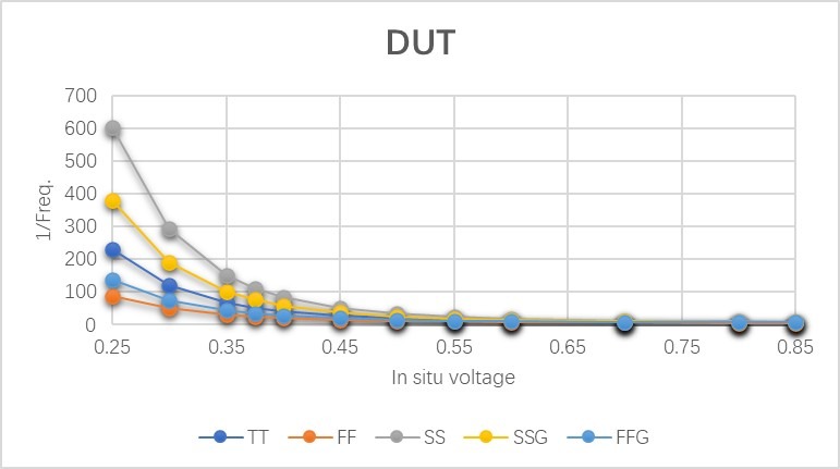
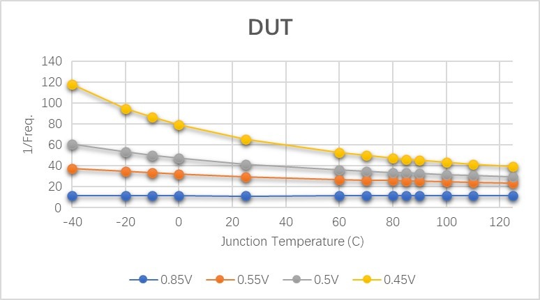
Combining the Performance Monitoring Element with the Process Monitoring Analysis Platform, through the serial output port of the chip, Extract the internal performance data of various chips before, after, and even during system operation to achieve chip design optimization, process improvement, product classification, and performance and lifetime analysis.

Variable parameters that affect chip performance
1
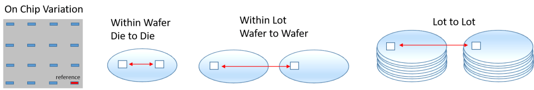
Process Variation
– On Chip Variation (within-die OCV)
– Global Variation (Die-to-Die, Wafer-to-Wafer, Lot-to-Lot)
2
Process Variation (制程差异)
– Static & Dynamic IR drop
– Within Chip, Off-Chip
3
Operating Temperature Variation
(温度差异)
4

Aging Effect (芯片老化)
DTCO方法

The new generation of semiconductor processes is becoming more and more complex, and more and more process parameters need to be adjusted. Because semiconductor processes are provided to different customers, DTCO uses customers' specific designs to examine the variation of PVT on chips, and provides the direction for wafer fab to evaluate and adjust process parameters. Therefore, DTCO enables the corresponding circuit design and process optimization to maximize the process advantages brought by advanced semiconductor nodes to the chip.
With experts from TSMC and Intel in DTCO, Lingyange is one of the few companies capable of providing DTCO chip design services in China, and is a leader in the industry.